NCP1606
http://onsemi.com
13
out the bulk voltage ripple, then this on time is truly
constant over the ac line cycle.
Note that the maximum on time of the controller occurs
when V
CONTROL
is at its maximum. Therefore, the Ct
capacitor must be sized to ensure that the required on time
can be delivered at full power and the lowest input voltage
condition. The maximum on time is given by:
t
ON(max)
+
Ct @ V
CTMAX
I
CHARGE
(eq. 4)
Combining this equation with equation 1, gives:
Ct w
2 @ P
OUT
@ L @ I
CHARGE
h @ Vac
RMS
2
@ V
CTMAX
(eq. 5)
where V
CTMAX
= 2.9 V (min)
I
CHARGE
= 297 mA (max)
OFF TIME SEQUENCE
While the on time is constant across the ac cycle, the off
time in CRM operation varies with the instantaneous input
voltage. The NCP1606 determines the correct off time by
sensing the inductor voltage. When the inductor current
drops to zero, the drain voltage (
Vd
in Figure 23) is
essentially floating and naturally begins to drop. If the
switch is turned on at this moment, then CRM operation
will be achieved. To measure this high voltage directly on
the inductor is generally not economical or practical.
Rather, a smaller winding is taken off of the boost inductor.
This winding, called the zero current detector (ZCD)
winding, gives a scaled version of the inductor output and
is more useful to the controller.
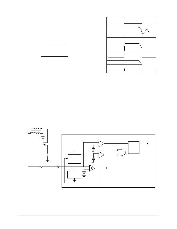
Figure 28. Voltage Waveforms for Zero Current
Detection
DRIVE
Winding
Pin
Drain
0.6 V
V
OUT
5.7 V
2.1 V
1.6 V
ZCD
Figure 28 gives typical operating waveforms with the
ZCD winding. When the drive is on, a negative voltage
appears on the ZCD winding. And when the drive is off, a
positive voltage appears. When the inductor current drops
to zero, then the ZCD voltage falls and starts to ring around
zero volts. The NCP1606 detects this falling edge and starts
the next driver on time. To ensure that a ZCD event has
truly occurred, the NCP1606s logic (Figure 29) waits for
the ZCD pin voltage to rise above V
ZCDH
(2.1 V typical)
and then fall below V
ZCDL
(1.6 V typical). In this way,
CRM operation is easily achieved.
Figure 29. Implementation of the ZCD Winding
ZCD
+
200 mV
+
2.1 v
VCL(POS)
Clamp
Shutdown
Demag
VCL(NEG)
Active
Clamp
+
1.6 V
Reset
Dominant
Latch
R
Q
S
DRIVE
R
SENSE
R
ZCD
V
DD
V
in
N
ZCD
Q
N
B
发布紧急采购,3分钟左右您将得到回复。
相关PDF资料
NCP1607BDR2G
IC PFC CONTROLLER CRM 8SOIC
NCP1611BDR2G
IC PFC CTLR HE ENHANCED 8-SOIC
NCP1651DR2G
IC PFC CONTROLLER CCM/DCM 16SOIC
NCP1654BD133R2G
IC PFC CCM 133KHZ 8-SOIC
NCP1927DR2G
IC CTLR PFC/FLYBACK 16-SOIC
NCP380HMU21AATBG
IC CURRENT LIMIT SWITCH 6-UDFN
NCT1008DMT3R2G
TMP DIO MON/SMBUS 4CH 8WDFN
NCT210RQR2G
IC TEMP SENSOR LOC/REM 16QSOP
相关代理商/技术参数
NCP1606BOOSTGEVB
功能描述:电源管理IC开发工具 OSPI NCP1606 100 W BOOST
RoHS:否 制造商:Maxim Integrated 产品:Evaluation Kits 类型:Battery Management 工具用于评估:MAX17710GB 输入电压: 输出电压:1.8 V
NCP1606BPG
功能描述:功率因数校正 IC LO CST PWR FCTR CONT RoHS:否 制造商:Fairchild Semiconductor 开关频率:300 KHz 最大功率耗散: 最大工作温度:+ 125 C 安装风格:SMD/SMT 封装 / 箱体:SOIC-8 封装:Reel
NCP1607BDR2G
功能描述:功率因数校正 IC CST EFCT PW FCTR CTR RoHS:否 制造商:Fairchild Semiconductor 开关频率:300 KHz 最大功率耗散: 最大工作温度:+ 125 C 安装风格:SMD/SMT 封装 / 箱体:SOIC-8 封装:Reel
NCP1607BOOSTGEVB
功能描述:BOARD EVAL NCP1607 100W BOOST RoHS:是 类别:编程器,开发系统 >> 评估演示板和套件 系列:* 标准包装:1 系列:PCI Express® (PCIe) 主要目的:接口,收发器,PCI Express 嵌入式:- 已用 IC / 零件:DS80PCI800 主要属性:- 次要属性:- 已供物品:板
NCP1608BDR2G
功能描述:功率因数校正 IC COST EFFECT PWR FACT CONT RoHS:否 制造商:Fairchild Semiconductor 开关频率:300 KHz 最大功率耗散: 最大工作温度:+ 125 C 安装风格:SMD/SMT 封装 / 箱体:SOIC-8 封装:Reel
NCP1608BOOSTGEVB
功能描述:电源管理IC开发工具 NCP1608 100 W BOOST EVB PWR SPY
RoHS:否 制造商:Maxim Integrated 产品:Evaluation Kits 类型:Battery Management 工具用于评估:MAX17710GB 输入电压: 输出电压:1.8 V
NCP1611ADR2G
功能描述:功率因数校正 IC NCP1611A ENHANCED PFC
RoHS:否 制造商:Fairchild Semiconductor 开关频率:300 KHz 最大功率耗散: 最大工作温度:+ 125 C 安装风格:SMD/SMT 封装 / 箱体:SOIC-8 封装:Reel
NCP1611BDR2G
功能描述:功率因数校正 IC NCP1611A ENHANCED PFC RoHS:否 制造商:Fairchild Semiconductor 开关频率:300 KHz 最大功率耗散: 最大工作温度:+ 125 C 安装风格:SMD/SMT 封装 / 箱体:SOIC-8 封装:Reel